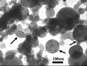
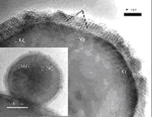
The structure, atomic and crystallographic, as well as the microstructure of a material, determine the physical properties of the material. The characterization of a material is therefore of considerable importance. A solid is an aggregate of randomly oriented grains of crystal. A crystal grain is a regular array of one or more types of atoms. The disruption of the arrangement of atoms in a crystal results in a crystal defect. Material characterization involves the identification of the atoms, their crystallographic structure and the microstructure of the target solid. An element is usually identified by its characteristic X-ray spectrum. Crystal structure is often determined by X-ray or electron diffraction. The characterization of a small grain, especially nanocrystalline grain, requires a probe of nanometer size. The transmission electron microscope (TEM) is the only instrument capable of providing chemical and structural (atomic and crystallographic) data for the characterization of a solid with high spatial resolution. By focusing a nanometer probe of electrons onto a small grain in a TEM, characteristic X-ray and diffraction pattern are generated. The detection and analysis of X-ray by means of Energy Dispersive Spectroscopy (EDS) in a TEM allows the identity and amount of the elements in the solid to be determined. Electron diffraction provides a means for the identification and determination of crystal orientation and structure. Imaging, the ultimate goal of microscopy, can be carried out in different ways depending on the occasion. Diffraction contrast imaging is usually used for the determination of crystal defects. High resolution TEM imaging is used for the observation of the atomic arrangement in the crystal.
Continue reading Structural analysis of crystalline and nanocrystalline materials


