The structure, atomic and crystallographic, as well as the microstructure of a material, determine the physical properties of the material. The characterization of a material is therefore of considerable importance. A solid is an aggregate of randomly oriented grains of crystal. A crystal grain is a regular array of one or more types of atoms. The disruption of the arrangement of atoms in a crystal results in a crystal defect. Material characterization involves the identification of the atoms, their crystallographic structure and the microstructure of the target solid. An element is usually identified by its characteristic X-ray spectrum. Crystal structure is often determined by X-ray or electron diffraction. The characterization of a small grain, especially nanocrystalline grain, requires a probe of nanometer size. The transmission electron microscope (TEM) is the only instrument capable of providing chemical and structural (atomic and crystallographic) data for the characterization of a solid with high spatial resolution. By focusing a nanometer probe of electrons onto a small grain in a TEM, characteristic X-ray and diffraction pattern are generated. The detection and analysis of X-ray by means of Energy Dispersive Spectroscopy (EDS) in a TEM allows the identity and amount of the elements in the solid to be determined. Electron diffraction provides a means for the identification and determination of crystal orientation and structure. Imaging, the ultimate goal of microscopy, can be carried out in different ways depending on the occasion. Diffraction contrast imaging is usually used for the determination of crystal defects. High resolution TEM imaging is used for the observation of the atomic arrangement in the crystal.
High resolution transmission electron microscopy (HRTEM) of passive epitaxial oxide films on nanocrystals of chromium and iron
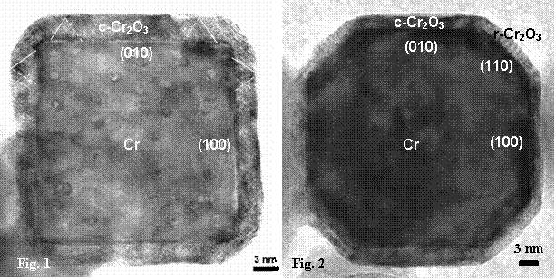
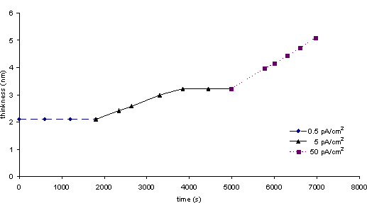
Nanocrystals of metals prepared by Prof. Qin of Tianjin University are remarkably oxidation and corrosion resistant. Nanocrystals of iron remain “rust free” in air and water for years. The size of these nanocrystals ranges from 20 nm to 400 nm. Electron diffraction and high resolution transmission electron microscopy (HRTEM) have shown that the nanocrystals of chromium and iron are protected by polyhedral epitaxial passive oxide films. Nanoparticles of chromium are truncated rhombic dodecahedra with  and
and  facets. Nanocubes with facets are obtained when the truncation is 100%. The nanocubes of chromium are passivated by an epitaxial face-centred cubic Cr2O3 shell (labelled c-Cr2O3 in Fig.1). The same cubic Cr2O3 is observed on the facets of partially truncated nanoparticles of Cr. But the epitaxial oxide film on the facets is the usual rhombohedral a-Cr2O3 (labelled r-Cr2O3 in Fig. 2). Similarly, the epitaxial oxide film on the facets of nanoparticles of Fe is cubic g-Fe2O3 while the oxide film on the facets is rhombohedral a-Cr2O3. Both the cubic and rhombohedral Cr2O3/Fe2O3 have been found to be effective in protecting the nanoparticle from further oxidation. The protection of bulk Cr and Fe by rhombohedral a-Cr2O3 is well known. We have previously shown that nanoparticles of Fe are protected by epitaxial g-Fe2O3. We have shown that nanoparticles of Cr and Fe are also protected by cubic Cr2O3 and a-Fe2O3. These results may have important implications for protective oxide films involving Cr and Fe.
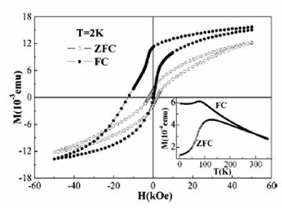
The stability of the oxide shell in nanoparticles of Cr and Fe against further oxidation has also been studied by electron beam heating in a transmission electron microscope. When the beam current is increased by one order of magnitude, the thickness of the epitaxial oxide on Cr nanoparticles increases from 2.0 nm to a self limiting value of 3.2 nm. When the beam current is increased again by an order of magnitude, the growth of the oxide film resumes and linear growth takes place (Fig. 3).
Due to the large size distribution, it has not been possible to determine the physical properties of these nanoparticles.
Publications:
- J.C. Rao, X.X. Zhang, B. Qin and K.K. Fung, “High-resolution transmission electron microscopy study of epitaxial passive films on nanocubes of chromium”, Philo. Mag. Lett., 83, 395-401 (2003).
- J.C. Rao, X.X. Zhang, B. Qin and K.K. Fung, “TEM study of the dependence of the epitaxial passive oxide films on crystal facets in polyhedral nanoparticles of chromium”, Ultramicroscopy 98., 231-238 (2004).
Exchange-bias field of core-shell structured mono-sized nanoparticles of Co and Fe
In order to study the magnetic properties of nanoparticles, mono-sized nanoparticles of Co (about 20 nm) and Fe (about 11 nm) have been fabricated in our size-selective gas condensation system. We have found that the nanoparticles are passivated by an oxide shell of about 3 nm in thickness. It is expected that the coupling between the antiferromagnetic oxide shell and the ferromagnetic metal core will result in an exchange bias effect. Large or giant exchange bias field has indeed been observed in the Co and Fe nanoparticles (Fig. 4). We have also found and successfully explained the decrease of exchange bias in nanoparticles of Fe in consecutive hysteresis loop measurements after field cooling.
Publications:
- R.K. Zheng, G.H. Wen, K.K. Fung & X.X. Zhang, “Giant exchange bias and the vertical shifts of the hysteresis loops in γ-Fe2O3 -coated Fe nanoparticles”, J. Appl. Phys 95, 5244-5246 (2004).
- R.K.Zheng, G.H. Wen, K.K. Fung and X.X. Zhang, “Training effect of exchange bias in γ-Fe2O3 coated Fe nanoparticles”, Phys. Rev. B.69, 214431-214434 (2004).
Structural colors in insects
Coloration in nature is based either on chemical pigments or physical structures, or a combination of structures and pigments. Example of pigmentary and structural colors is illustrated by the colors of the scales of a Paris peacock butterfly shown in Fig. 5. The duller red and black colors are due to pigments. The brighter and iridescent blue color is due to structure. Iridescent structural colors can easily be observed in the wings and bodies of many butterflies, beetles and birds. The structural colors of silverfish (an insect) and peacock feathers were recognized respectively by Hooke in 1665 and Newton in 1730. The reflection of circularly polarized light from the cuticules of scarab beetles was first reported by Michelson in 1911. The most common light reflection physical structure is the multilayer reflector which consists of a stack of quarter-wavelength layers of alternating high refractive chitin and low refractive air. The thickness of the chitin layers is usually below 100 nm. It is now clearly recognized that multilayer reflectors, diffraction gratings and other optical inventions have existed naturally for millions of years before they were invented by scientists. When a wing is covered instead by an array of nanometer protuberances, 200 nm in diameter and height, reflection is reduced to zero and the wing becomes transparent. Such an array, first observed on the eyes of moths, is known as moth-eye structure. The moth-eye structure has been replicated as antireflection covering on solar cells. The multilayer structure is an example of one-dimensional photonic structures. Recently, iridescence arising from two-dimensional photonic structure consisting of hexagonal array of cylindrical tubes of air in chitin has been observed in an aquatic animal.
Hong Kong is well known for her biodiversity, with over 4,000 species of insects and 238 species of butterflies. We have initiated preliminary studies on local butterflies, moths and a bee in a number of undergraduate research projects using optical microscopy and spectroscopy, and scanning and transmission electron microscopy.
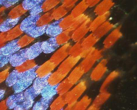
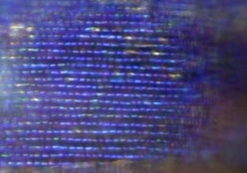
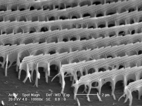
Fig. 5 shows that the iridescent blue is observed in localized areas on the scale rather than the whole scale. The localization of iridescent color is more clearly shown in the wing scale of an Euploeini butterfly in Fig. 6. The iridescent elongated blue spots are localized on the ridges of the wing scale. The multilayer structure of the ridges is clearly visible in the scanning electron microscope image in Fig. 7. The array of blue linear spots corresponds to the steps on the inclined multilayers. The inclined ridge multilayers on the wing scales result in the flashing of the blue color such that the color can be seen or disappear suddenly when the direction of observation is changed.
References:
- Parker, “515 million years of structural colour”, J. Opt. A 2, R15-R28 (2000).
- Vukusic and J.R. Sambles, “Photonic structures in biology”, Nature 424, 852-855 (2003).A.R.