Photonic band gaps can be generally classified into two main categories: Bragg gap or resonance gap. For the Bragg gap, a dielectric mirror formed by stacking two different types of dielectrics in alternative sequence is a very good representative. This kind of gap is formed from Bragg scattering arising from the periodicity. For the resonance gap, photonic crystals formed from placing metallic spheres periodically inside a dielectric is also a good representative. The kind of gap is formed from the resonance of a single sphere. In this work, we found that there is an additional mechanism in forming photonic band gap if we can also have a double negative (DNG) medium in designing photonic crystals.
When we stack two different kinds of dielectrics in one direction, the Bragg condition can be expressed in very simple terms by the total optical path elapsed through one unit cell. If this optical path equals to p, 2p, 3p, etc., a Bragg gap is opened. The optical path elapsed is always positive in ordinary situations. However, if we can also have DNG material being one kind of material in the stacking, there is an extra possibility that the optical path can be completely cancelled out to zero as a DNG material posses a negative refractive index. It can be expressed mathematically by  , where
  is the refractive index and
  is the thickness of the two different types of slabs. At this situation, a photonic band gap also opens and we call it a zero- n gap. As optical path is proportional to frequency, a Bragg gap shifts in frequency but a zero-n gap is invariant upon a change of scale length. Moreover, the zero-n gap is also insensitive to disorder that can maintain a zero n on average. This work has been published in Phys. Rev. Lett. 90, 083901.
 and
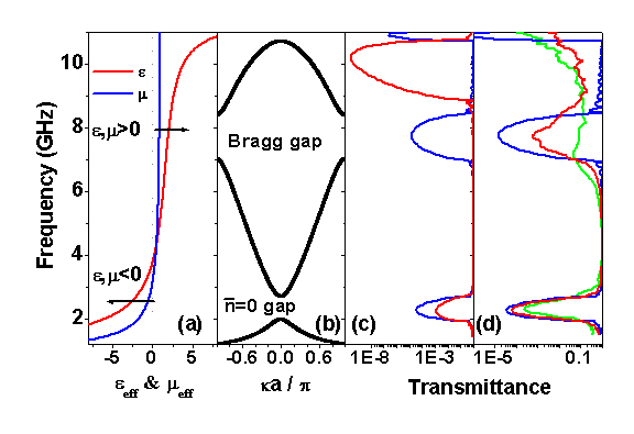
and  as the functions of frequency of a designed negative-n material, with structural details shown in the inset; (b) Band structure for a photonic crystal with alternating layers of air and the designed negative-n material; (c) Transmittance through a slab consisting of 16 unit cells through direct FDTD simulation (solid line) and material properties represented by and (open circles).
 and
and  of the negative-n material, as given; (b) Dispersion relationship of a photonic crystal with alternate layers of air and the negative-n material with material parameter as shown in (a); (c) Blue curve: Transmittance through 16 unit cells, corresponding to the band structure in (b). Red curve: Transmittance when the lattice constant is scaled by 2/3; (d) Transmittance through 16 unit cells, with various degree of disorder in thickness.